-Virtual Reactor: Optimization: Reactor geometry and growth process parameters MOCVD : III-V and III-N thin film growth optimization 2D Simulation HVPE: GaN bulk and GaN thin film growth optimization 2D Simulation -CVDSim NE: add on 3D Simulation coupled with FLUENT and CFD Ace+: -STREEM: Strain&Dislocation Engineering Simulation of AlGaN and InGaN material -SimuLED(SiLENSe(2D-epi:LED/LD),SpeCLED(3D chip), RATRO(3D ray tracing)): LED Simulation -SimuLamp: LED Package level 3D Simulation -FETIS: Field Effect Transistor Simulation -PVCell: Semiconductor Photo Voltaic Cell Simulation -BESST: Bandgap Engineering Superlattice Simulation Tool
Hardware (Nano Materials and Device)
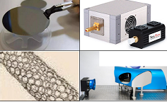
-Nano particles: SWCNT, MWCNT, Graphene, Nano powder -Semiconductor wafers: Substrate and epi wafer with III-V and III-N -NDT(Non Destructive Testing) Device: -Sub-THz and THz 2D&3D image Scanner system: Radar system
S244-ho, 31th floor, A-dong, 323 IncheonTower-daero, Yeonsu-gu, Incheon-si, 22007, Republic of korea Tel : +82-32-612-8252 / Fax : +82-32-232-0431 / E-mail ; noniess@infotc.co.kr or noniess@naver.com copyright 2023 infotech, All Rights Reserved.